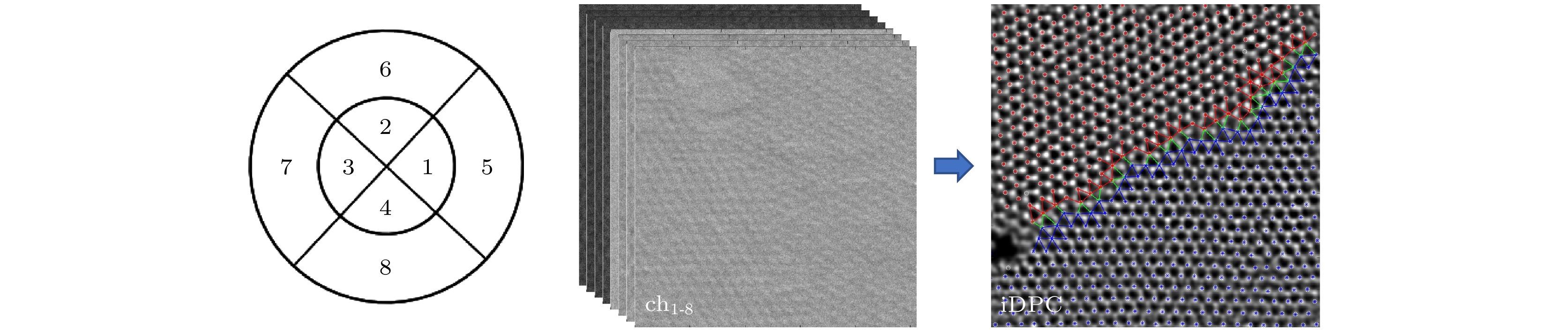
Two-dimensional planar heterojunctions composed of single-layer transition metal dichalcogenides have great potential applications in low-power, high-performance, and flexible optoelectronic devices. The localized atomic structure and crystal defects at interface govern the electronic, magnetic, optical, catalytic, and topological quantum properties. However, accurate characterization of interface atomic structure is still a challenge, so far. To determine the accurate atomic position, a spherical aberration-corrected electron microscope with segmented detector is employed, and the calculation is performed by integrated differential phase contrast (iDPC) imaging algorithm. By using the iDPC method, the atomic structure of WS2-MoSe2 monolayer heterojunction interface is characterized, and the W, Se, Mo, and S atoms are imaged simultaneously. Statistics show that the angles between the lattices on both sides of the WS2-MoSe2 planar heterojunction are distributed around 29° and 35°. Additionally, it is found that the lattice near the boundary experiences the strains of approximately 4‰ and 2% in the two lattice vector directions, with significant distortion occurring only at the interface. In this work, several typical atomic configurations, including merge type, quadrilateral type, and pentagonal type are found. The interface atomic configuration can help to release stress at the lateral interface. This study provides a useful method for accurately characterizing the structures for planar heterojunctions of monolayer transition metal dichalcogenide. It is of great significance for in-depth research on the structure-property relationship at single-atom resolution in various interface structures.


 下载:
下载:


