


-
光电子技术领域的快速发展对半导体材料在光电特性上提出了更高要求, 推动了对更加高效、可控的调控手段的深入探索. 高压技术作为一种“干净”的外场调控手段, 能够有效地调控材料晶体结构与电子态, 激发新奇物理现象, 实现性能的优化. 近年来, 高压技术在光电功能材料领域迅速崭露头角, 为光电特性的优化提供了全新视角, 展现出不俗的研究价值和应用潜力. 本文概述了近年来二维过渡金属硫化物、金属与非金属卤化物等材料体系在高压条件下光电响应特性演化的研究进展. 总结了高压对材料晶体结构、电子能带、光谱响应拓展、自驱动响应、极性反转等效应的影响规律, 分析了结构与性能的内在关联, 并探讨了高压调控所揭示的新机制和新效应. 最后, 针对当前压力调控光电特性领域存在的科学问题与技术瓶颈, 提出了未来可能的研究方向与前景, 以期为开发新型高性能光电器件提供理论基础和实验依据.
The rapid development of optoelectronic technologies has raised increasingly requirements for the photoelectric properties of semiconductor materials, thereby promoting the exploration of more efficient and controllable modulation strategies. High-pressure technology, as a clean and effective external-field method, can accurately modulate the crystal structure and electronic states of materials. This modulation can induce novel phase transitions and physical effects, thereby significantly improving performance. In recent years, high-pressure technique has emerged as a powerful tool for optimizing photoelectric properties of semiconductor materials, providing new perspectives for enhancing performance and demonstrating significant research value and application potential. This review paper comprehensively summarizes recent research progress of pressure-induced evolution of photoelectric properties in various material systems, such as two-dimensional transition metal dichalcogenides, metal and non-metal halides, perovskites, and other representative semiconductors. These materials exhibit a wide variety of pressure-induced structural transformations, accompanied by photocurrent enhancement, broadband spectral response, self-powered photoresponse, and polarity reversal. Furthermore, the intrinsic links between these structural evolutions and the corresponding photoelectric behaviors are systematically examined. Scientific issues and development bottlenecks in this area are also discussed. Despite notable advances, there are still several challenges, including the insufficient understanding of intrinsic correlations between structure and photoelectric properties, the lack of comprehensive evaluation parameters. How to realize pressure-enhanced photoelectric properties for applications under ambient conditions is another key challenge. Addressing these issues will be essential for advancing both fundamental understanding and practical applications. Overall, pressure modulated photoelectric properties present both significant challenges and exciting opportunities, providing valuable guidance for designing advanced optoelectronic materials and devices. 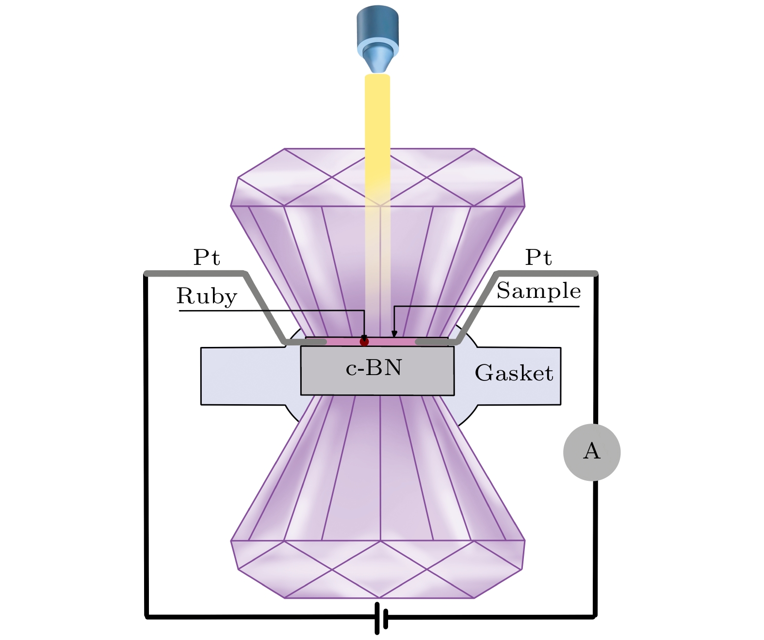
-
Keywords:
- high-pressure physics /
- photoresponse characteristics /
- structural phase transition /
- in-situ high-pressure characterization
[1] [2] [3] [4] [5] [6] [7] [8] [9] [10] [11] [12] [13] [14] [15] [16] [17] [18] [19] [20] [21] [22] [23] [24] [25] [26] [27] [28] [29] [30] [31] [32] [33] [34] [35] [36] [37] [38] [39] [40] [41] [42] [43] [44] [45] [46] [47] [48] [49] [50] [51] [52] [53] [54] [55] [56] [57] [58] [59] [60] [61] [62] [63] [64] [65] [66] [67] [68] [69] [70] [71] [72] [73] [74] [75] [76] [77] [78] [79] [80] [81] [82] [83] [84] -
材料名称 压力范围/GPa 光电流较常压数值 其他现象 参考文献 多层MoS2 0—35.0 — 光电流增益–7.5%/GPa、金属化 [40] PtS2 0—26.8 约6倍 — [41] 块状ReS2 0—50.0 2个数量级 金属化 [42] WS2 0—17.2 2个数量级 宽谱响应 [43] ZrSe2 0—26.5 3个数量级 金属化、负光电导 [44] PbI2 0—32.6 2个数量级 宽谱响应、自驱动光响应 [46,47] BiI3 0—30.0 3个数量级 宽谱响应、自驱动光响应 [48] SbI3 0—10.0 近10倍 自驱动光响应 [49,50] CsI3 0—16.7 近5个数量级 宽谱响应 [51] SnI4 0—11.5 约5个数量级 金属化 [52] RhI3 0—30.0 约5个数量级 金属化 [53] AsI3 0—12.0 约2倍 — [54] (C6H5CH2NH3)2CuBr4 0—40.0 28 GPa光电导率达到峰值* — [55] Cs2PbI2Cl2 0—26.9 3个数量级 — [24] CH3NH3PbBr3 0—5.6 0.7 GPa达到峰值* — [56] CH3NH3PbI3 0—8.3 4.5倍 “记忆效应” [57] CsPbBr3 0—9.2 1.4 GPa达到峰值* — [58] CsPbCl3 0—22.1 近2倍 — [59] CH3NH3SnI3 0—31.0 约1—2个数量级 非晶化 [60] Cs3Bi2I9 0—26.7 5个数量级 非晶化、宽谱响应 [61] NbOI2 0—23.8 3个数量级 宽谱响应、导电类型切换 [62] SbSI 0—28.5 14 GPa达到峰值* 自驱动光响应 [63] g-C3N4 0—46.0 约50% 带隙减小、非晶化、“记忆效应” [66,67] CuInP2S6 0—23.5 2个数量级 金属化、自驱动光响应 [68] NiPS3 0—50.1 5个数量级 宽谱响应、“记忆效应” [69] Bi9O7.5S6 0—58.1 4个数量级 — [70] BiOBr 0—25.0 1个数量级 — [71] KBiFe2O5 0—35.0 2个数量级 — [72] WO3/CuO异质结 0—33.0 — 负光电导 [73] CrSb2 0—41.0 — 负光电导 [74] Cr2Se3 0—31.8 3.7倍 负光电导 [75] 块状Si 0—20.8 1—2个数量级 金属化、负光电导 [76] CuInS2纳米晶 0—50.2 近4倍 带隙增大 [77] Bi2S3 0—34.3 5.6倍 宽谱响应、负光电导 [84] 注: *代表文献中未提及光电流具体变化数值.  下载: 导出CSV
-
[1] [2] [3] [4] [5] [6] [7] [8] [9] [10] [11] [12] [13] [14] [15] [16] [17] [18] [19] [20] [21] [22] [23] [24] [25] [26] [27] [28] [29] [30] [31] [32] [33] [34] [35] [36] [37] [38] [39] [40] [41] [42] [43] [44] [45] [46] [47] [48] [49] [50] [51] [52] [53] [54] [55] [56] [57] [58] [59] [60] [61] [62] [63] [64] [65] [66] [67] [68] [69] [70] [71] [72] [73] [74] [75] [76] [77] [78] [79] [80] [81] [82] [83] [84]


 下载:
下载:


计量
- 文章访问数: 1154
- PDF下载量: 38
- 被引次数: 0